

Semiconductor Packaging
Protect every wafer, die and substrate — from fab to final assembly.
Customer Challenges
Where static-sensitive, high-value devices are won or lost.
Semiconductor packaging fails quietly — in yield, uptime and audit. These are the pain points we engineer out.
ESD damage
Static-sensitive components fail or silently degrade during handling and transit.
Particulate & ionic contamination
Particles and ionic residue reduce yield and threaten downstream cleanliness.
Micro-damage
Chipping, scratches and coplanarity loss from poor nesting and handling.
Automation misfit
Trays that don't index reliably stall pick-and-place and assembly lines.
Long tooling lead time
Slow tooling delays device ramp and pushes out time-to-volume.
Supplier risk
Distant, single-source packaging adds lead-time and validation risk.
Konix Solution
ESD-controlled carriers, engineered and validated before volume.
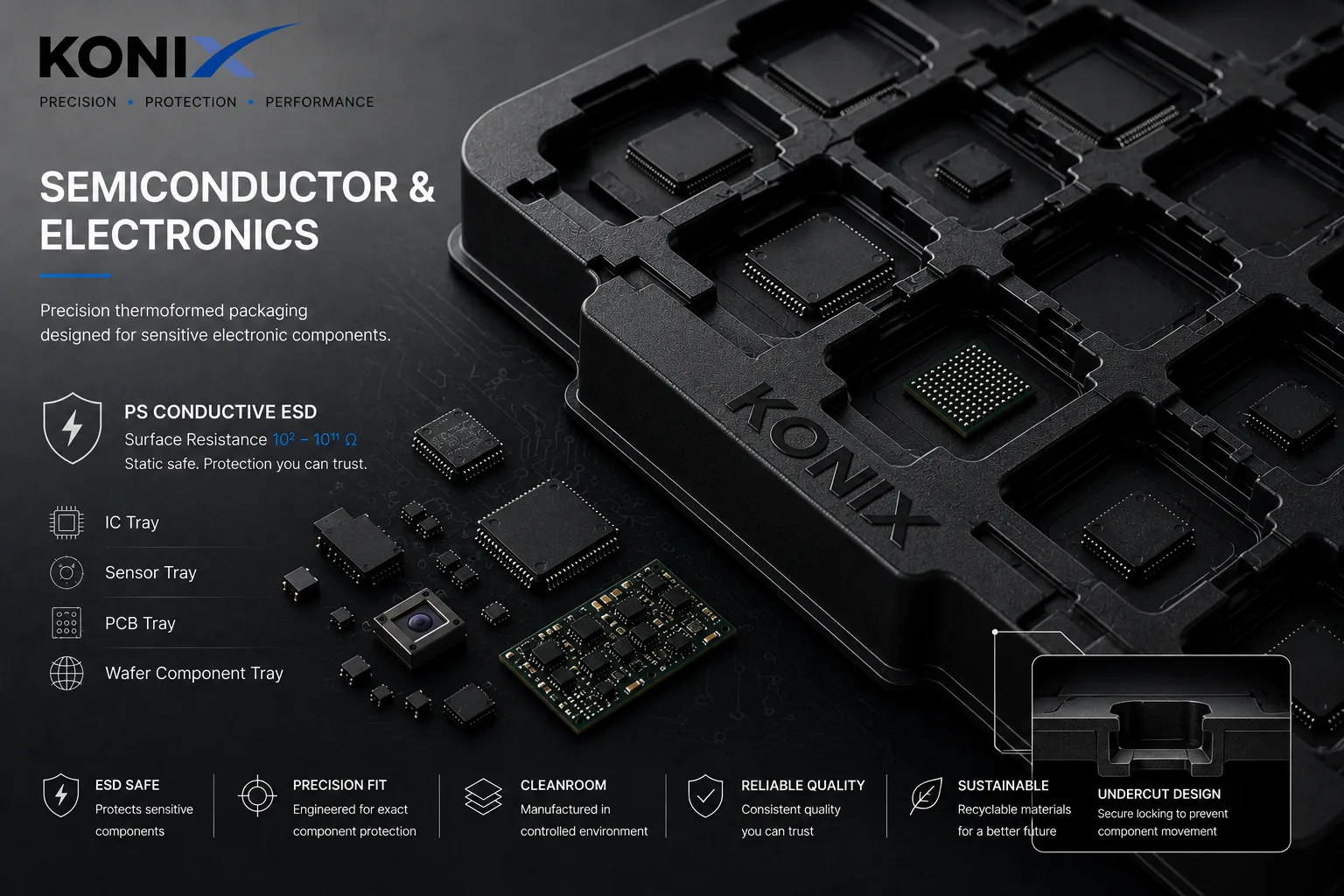
We design carriers, trays and shippers that are ESD-controlled and cleanroom-manufactured, shaped around your component geometry, automation and transit loop — then validate surface resistance and nesting before you commit to volume.
- Conductive / dissipative materials to defined surface-resistance targets.
- Cleanroom Class 8 & 9 manufacturing, cleaning and packing.
- Custom nesting that immobilises devices and indexes for automation.
- Surface-resistance and transit validation to your standard.
Applications
Formats we engineer for semiconductor.
Business Benefits
What it means for your KPIs.
Risk reduction
ESD and contamination controlled by design, lowering field-failure and yield risk.
Process / Quality engineerLower cost per unit
Right-sized, reusable formats reduce packaging spend over the device lifecycle.
PurchasingProcess improvement
Reliable indexing and nesting steady the line and cut tray-related stoppages.
ManufacturingManufacturability & speed
In-house tooling and DFM shorten time-to-volume and de-risk validation.
FDI / plant managerEngineering Features
The engineering behind the tray.
Surface-resistance targets
Conductive and dissipative materials specified and verified to your ESD requirement.
Cleanroom manufacturing
ISO Class 8 & 9 environments for forming, cleaning and packing.
Custom nesting
Geometry-specific pockets that immobilise devices and protect fragile features.
DFM co-design
We engineer with your team for fit to part, automation and transit.
Validation & testing
Surface-resistance, drop and transit validation before volume.
In-house tooling
CNC and soft-tool fabrication with secure, fire-protected mould storage.
Case Study
SiP launch — ESD rejects and line stoppages.
An IDM launching a System-in-Package faced ESD-related rejects and tray-driven line stoppages during ramp.
A co-designed dissipative carrier with validated surface resistivity and custom nesting, qualified before volume.
ESD-related rejects controlled · steadier line stability · lower packaging cost per unit.
Outcomes are directional and vary by device, geometry and validation scope. We model the expected result with you before tooling.
FAQ
Semiconductor packaging questions.
Can you hit a specific surface-resistance target?
Are parts cleanroom-manufactured?
Do your trays work with our automation?
What about tooling lead time?
Request a Solution
Protecting static-sensitive or high-value devices? Send us your part.
We'll propose an ESD-safe, validated solution — a recommendation, not a generic quote. A local engineering team in Đồng Nai. Your drawings and data stay confidential.